

The NTFM Group pioneers the atomic-scale design of functional thin films and 2D heterostructures through innovative synthesis, precision deposition, and advanced metrology. Their work spans superconducting nanocrystals, strain-resilient van der Waals heterostructures, high-k dielectrics, and multifunctional nanocomposites—enabling breakthroughs in flexible electronics, quantum devices, and sustainable materials.
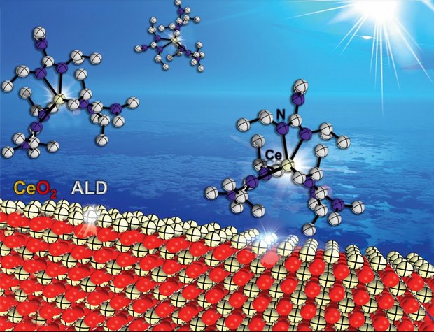
The Nanostructured Thin Film Materials (NTFM) group pursues a materials-by-design approach to engineer nanoscale functional systems through atomic-layer processing and chemical vapor deposition (CVD) techniques, including Metal-Organic CVD (MOCVD), Atomic Layer Deposition (ALD), and Area-Selective Deposition (ASD). Our research centers on the chemistry of thin-film growth, interface engineering, and phase control to tailor the electrical, optical, mechanical, and quantum properties of metal oxides, nitrides, sulfides, and 2D materials.
We specialize in the bottom-up synthesis of phase-pure 2D nanocrystals (e.g., 3R-TaSe₂, NbS₂), strain-resilient van der Waals heterostructures (e.g., CrCl₃/MoS₂), and multifunctional nanocomposites (e.g., MXene/aramid films) with applications in flexible electronics, quantum devices, EMI shielding, and advanced semiconductors.
By integrating in-situ and advanced ex-situ characterization (neutron scattering, electron microscopy, XPS), we uncover emergent phenomena such as superconductivity, anisotropic lattice dynamics, and surface reactivity.
We collaborate closely with universities, research institutes, chemical suppliers, and equipment manufacturers to develop novel precursors, validate scalable processes, and accelerate the transition from lab to industry.
Mission: To engineer next-generation functional nanomaterials through atomic-scale control of thin-film growth, interface design, and phase engineering — bridging fundamental science and scalable technology for electronics, quantum devices, and sustainable materials.
The aim of this initiative is to enable large-scale processing of advanced functional materials at the atomic level for future nanotechnologies. Therefore, the Competence Center at IFW Dresden has been upgraded with an industrial MOCVD reactor. This system enables highly precise process control, especially with newly developed precursors, greatly enhancing the institute’s materials research capabilities. In addition, a state-of-the-art atomic layer deposition (ALD) platform has been installed, providing advanced capabilities for the deposition of a wide range of material systems, including 2D materials, metals, and dielectric thin films on technologically relevant substrate sizes. The system is also compatible with custom-designed precursor compounds, creating new opportunities for process development and materials innovation. Together, these developments further strengthen the Competence Center’s role as a bridge between fundamental research and application-driven development.
The group pioneers thermodynamically guided and bottom-up synthesis strategies for novel 2D materials and nanocrystals. Key achievements include:
These works highlight a deep understanding of phase stability, nucleation kinetics, and interfacial interactions in low-dimensional systems.
A major focus is on designing and integrating 2D materials into functional heterostructures with tailored electronic and magnetic properties:
The group develops novel precursor chemistries and deposition techniques to enable high-quality, scalable thin films:
These advances support the integration of high-k dielectrics and functional oxides into nanoscale devices.
The group extends its expertise to hybrid and composite materials with enhanced performance:
Understanding surface reactivity is critical for device reliability:
The group integrates cutting-edge analytical techniques to probe structure, composition, and dynamics:
The NTFM Group’s work is driving innovation in:
With a strong emphasis on scalability, reproducibility, and industrial relevance—evidenced by work on 200 mm wafers and process optimization—the group bridges fundamental science and real-world applications.
“From atoms to devices — we design materials with purpose.”
— Dr. Harish Parala, NTFM Group
The NTFM Group thrives on interdisciplinary collaboration with:


