Description follows
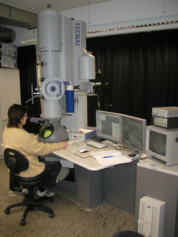
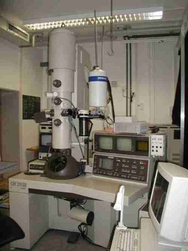
Operates at 300 kV accelerating voltage and is equipped with:
| Specimens: | Thickness 5 - 300 nm, diameter 3 mm |
|---|---|
| Holders: | Single tilt low background (+- 40° tilt), double tilt low background, double tilt low background with cooling (liquid N2), double tilt rotation holder, in-situ straining holder, in-situ STM holder |
| Resolution: | Point res. 0.19 nm, Information limit 0.12 nm |
| Magnification: | 70 x - 18 Mill. x |
| STEM: | Resolution 0.2 nm (Mag. up to 230 Mill. x) BF-, DF-, HAADF-detectors |
| EDXS: | Lateral resolution < 2 nm. Detection of all chemical elements with Z >= 5 (Bor), detection limit 0.5 %, correctness 20 % |
| EELS: | Lateral resolution < 1 nm. Energy resolution < 1 eV. Especially effective for light elements (e.g. B, C, N, O), detection limit very matrix dependent, >= 0.5 %, correctness 30 % |
| Energy filtered imaging: | Lateral resolution < 1 nm, energy resolution about 1 eV. |
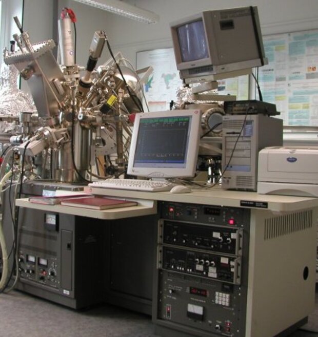
Operates at 200 kV accelerating voltage and is equipped with:

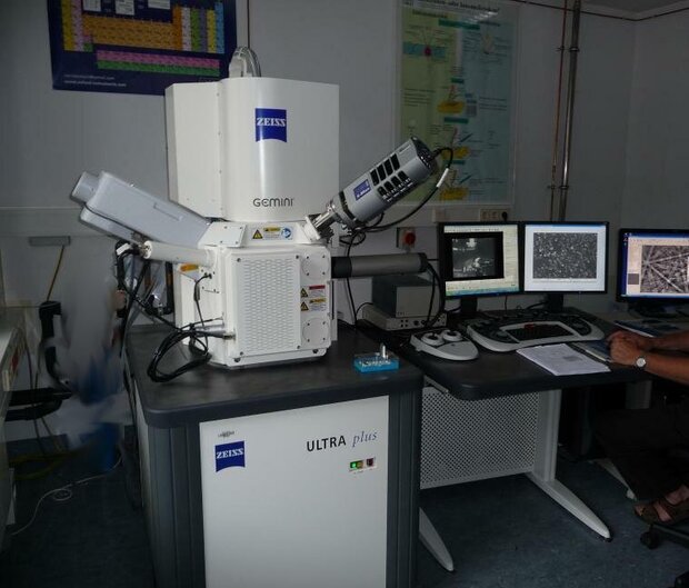
The Focussed Ion Beam (FIB) technology (FIB Helios 5 CX, ThermoScientific) is used for investigations in materials research or microelectronics, esp. for high contrast imaging of thin film microstructure using the channeling effect, cross section preparation, failure analysis, microstructuring, or thin film device modification. Using a focussed Gallium ion beam, it can precisely remove or deposit material at the sample surface on a submicron scale as well as image the sample surface or cross-section producing high quality contrast images with high magnifications.
The XPS system enables quantitative element analysis at surfaces of solid materials by spectroscopy of emitted photo electrons and gives information on the chemical states by analysis of peak-shifts or peak-shape changes.
System characteristics:


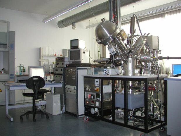


The deposition machine CARMEN is a versatile tool for various deposition techniques.
Chamber in the middle = handler for transfer and with three measurement stages (optical layer thickness, electrical sheet resistance method in construction)
Chamber 1 = load lock with hot carrier system (heating in all chambers except chamber 6)
Chamber 2 = ion beam pretreatment (Mark I+ Kaufman-type ion source) for surface preclean and etch applications with high-current, low-energy ions
Chamber 3 = DC magnetron co-sputtering of metallizations (Cu, Al, Ag, Ti, W, Co, Fe, Ni, Zr)
Chamber 4 = HF magnetron sputtering (reactive) of metallizations and barriers (Ti, Ru, Ta5Si3, TaSiN)
Chamber 5 = HF magnetron sputtering (reactive) of insulators (SAW-grade SiO2)
Chamber 6 = e-beam evaporation (Cu, Al, Ag, Au, Ti)
(From Thermo Scientific)
The Focussed Ion Beam (FIB) technology (FIB Helios 5 CX, Thermo Scientific) is used for investigations in materials research or microelectronics, esp. for high contrast imaging of thin film microstructure using the channeling effect, cross section preparation, failure analysis, microstructuring, or thin film device modification. Using a focussed Gallium ion beam, it can precisely remove or deposit material at the sample surface on a submicron scale as well as image the sample surface or cross-section producing high quality contrast images with high magnifications.
(From Fischione)
(Disco)
(Struers)
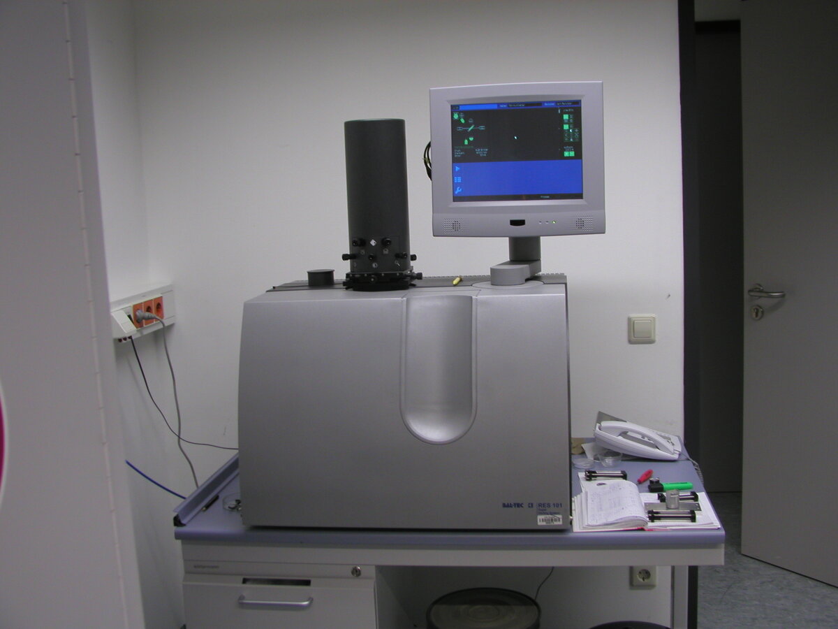
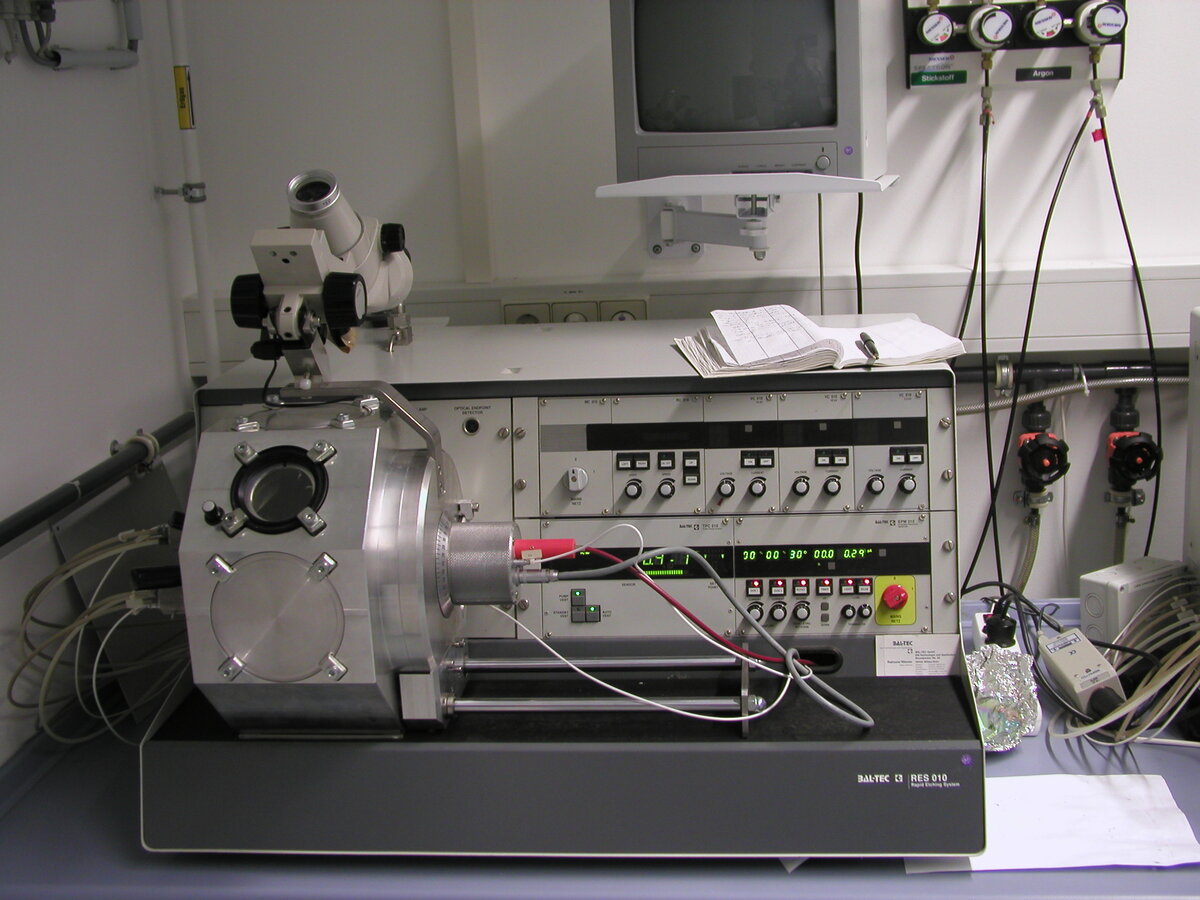
for removing contamination and ultra-low energy thinning with special sample holder
The deposition machine CARMEN is a versatile tool for various deposition techniques.
Chamber in the middle = handler for transfer and with three measurement stages (optical layer thickness, electrical sheet resistance method in construction)
Chamber 1 = load lock with hot carrier system (heating in all chambers except chamber 6)
Chamber 2 = ion beam pretreatment (Mark I+ Kaufman-type ion source) for surface preclean and etch applications with high-current, low-energy ions
Chamber 3 = DC magnetron co-sputtering of metallizations (Cu, Al, Ag, Ti, W, Co, Fe, Ni, Zr)
Chamber 4 = HF magnetron sputtering (reactive) of metallizations and barriers (Ti, Ru, Ta5Si3, TaSiN)
Chamber 5 = HF magnetron sputtering (reactive) of insulators (SAW-grade SiO2)
Chamber 6 = e-beam evaporation (Cu, Al, Ag, Au, Ti)
The XPS system enables quantitative element analysis at surfaces of solid materials by spectroscopy of emitted photo electrons and gives information on the chemical states by analysis of peak-shifts or peak-shape changes.
System characteristics:
(From Thermo Scientific)
The Focussed Ion Beam (FIB) technology (FIB Helios 5 CX, Thermo Scientific) is used for investigations in materials research or microelectronics, esp. for high contrast imaging of thin film microstructure using the channeling effect, cross section preparation, failure analysis, microstructuring, or thin film device modification. Using a focussed Gallium ion beam, it can precisely remove or deposit material at the sample surface on a submicron scale as well as image the sample surface or cross-section producing high quality contrast images with high magnifications.
Description follows
Operates at 300 kV accelerating voltage and is equipped with:
| Specimens: | Thickness 5 - 300 nm, diameter 3 mm |
|---|---|
| Holders: | Single tilt low background (+- 40° tilt), double tilt low background, double tilt low background with cooling (liquid N2), double tilt rotation holder, in-situ straining holder, in-situ STM holder |
| Resolution: | Point res. 0.19 nm, Information limit 0.12 nm |
| Magnification: | 70 x - 18 Mill. x |
| STEM: | Resolution 0.2 nm (Mag. up to 230 Mill. x) BF-, DF-, HAADF-detectors |
| EDXS: | Lateral resolution < 2 nm. Detection of all chemical elements with Z >= 5 (Bor), detection limit 0.5 %, correctness 20 % |
| EELS: | Lateral resolution < 1 nm. Energy resolution < 1 eV. Especially effective for light elements (e.g. B, C, N, O), detection limit very matrix dependent, >= 0.5 %, correctness 30 % |
| Energy filtered imaging: | Lateral resolution < 1 nm, energy resolution about 1 eV. |
Operates at 200 kV accelerating voltage and is equipped with:
The Focussed Ion Beam (FIB) technology (FIB Helios 5 CX, ThermoScientific) is used for investigations in materials research or microelectronics, esp. for high contrast imaging of thin film microstructure using the channeling effect, cross section preparation, failure analysis, microstructuring, or thin film device modification. Using a focussed Gallium ion beam, it can precisely remove or deposit material at the sample surface on a submicron scale as well as image the sample surface or cross-section producing high quality contrast images with high magnifications.
(From Fischione)
(Disco)
(Struers)
for removing contamination and ultra-low energy thinning with special sample holder
Tel.: +49 (351) 4659 298
Fax: +49 (351) 4659 9298
E-Mail: T.Gemming(at)ifw-dresden.de
Postal Delivery:
Dr. T. Gemming, IFW Dresden, Helmholtzstr. 20, 01069 DRESDEN, GERMANY
Visitors:
Helmholtzstr. 20, 01069 Dresden, Room A EG.03.1 (Main building, main entrance, turn left, 3rd door)