
In microelectronic devices failures can occur which are due to migration effects in interconnects or metallizations. This is especially the case for high electric current densities in modern devices. The migration effects include transport of mass which is accompanied by internal stresses. To understand the mechanisms of these effects it is necessary to measure the strain state of the individual grains of the metallizations. This requires a method to determine the strain with a spatial resolution better than 0.1 µm, which is currently not attainable by X-ray based methods.
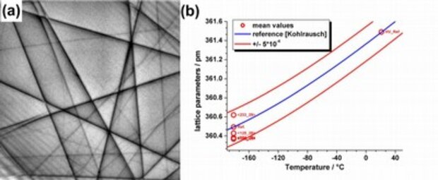
With convergent beam electron diffraction (CBED) in the transmission electron microscope (TEM) we succeeded to determine lattice parameters of Al and Cu with the required spatial resolution. The measurement is based on the evaluation of the position of defect lines in the diffraction discs, which originate from higher order Laue-zones (Fig. 1a). A lattice parameter determination of materials like Al and Cu requires the evaluation of the dynamical effects in the electron diffraction to achieve the necessary accuracy for strain determination.
Reference measurements of the thermal expansion of Al and Cu were carried out to demonstrate the applicability of the method (Fig. 1b). The errors of the obtained lattice parameters could be determined to be below 5×10⁻⁴, which is sufficient to evaluate stress components in structured metallizations like interconnect lines.


