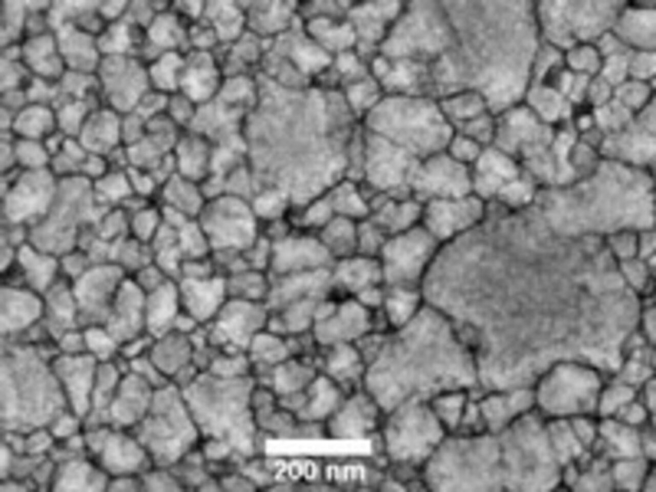
The IFW Dresden has extensive and long-term expertise in the field of scanning electron microscopy (SEM) and related analysis methods at its disposal. In addition, modern transmission electron microscopy (TEM) is used to visualize and characterize structural changes in materials in the nanometer range. In addition, the scientists can use spectroscopic methods such as energy dispersive X-ray spectroscopy (EDXS) and electron energy loss spectroscopy (EELS and ELNES). Various in-situ experiments can also be realised with electron microscopy.
Moreover, necessary techniques for sample preparation are part of our service portfolio, so that the entire material analysis can be taken over by the institute.