In-house production of two-layer plated-through circuit boards is possible up to a structure width of 100 µm. Chemical tin and solder resist mask can be realized as finishes. The structuring is done either by milling or conventionally wet-chemical with direct exposure or by film processing.

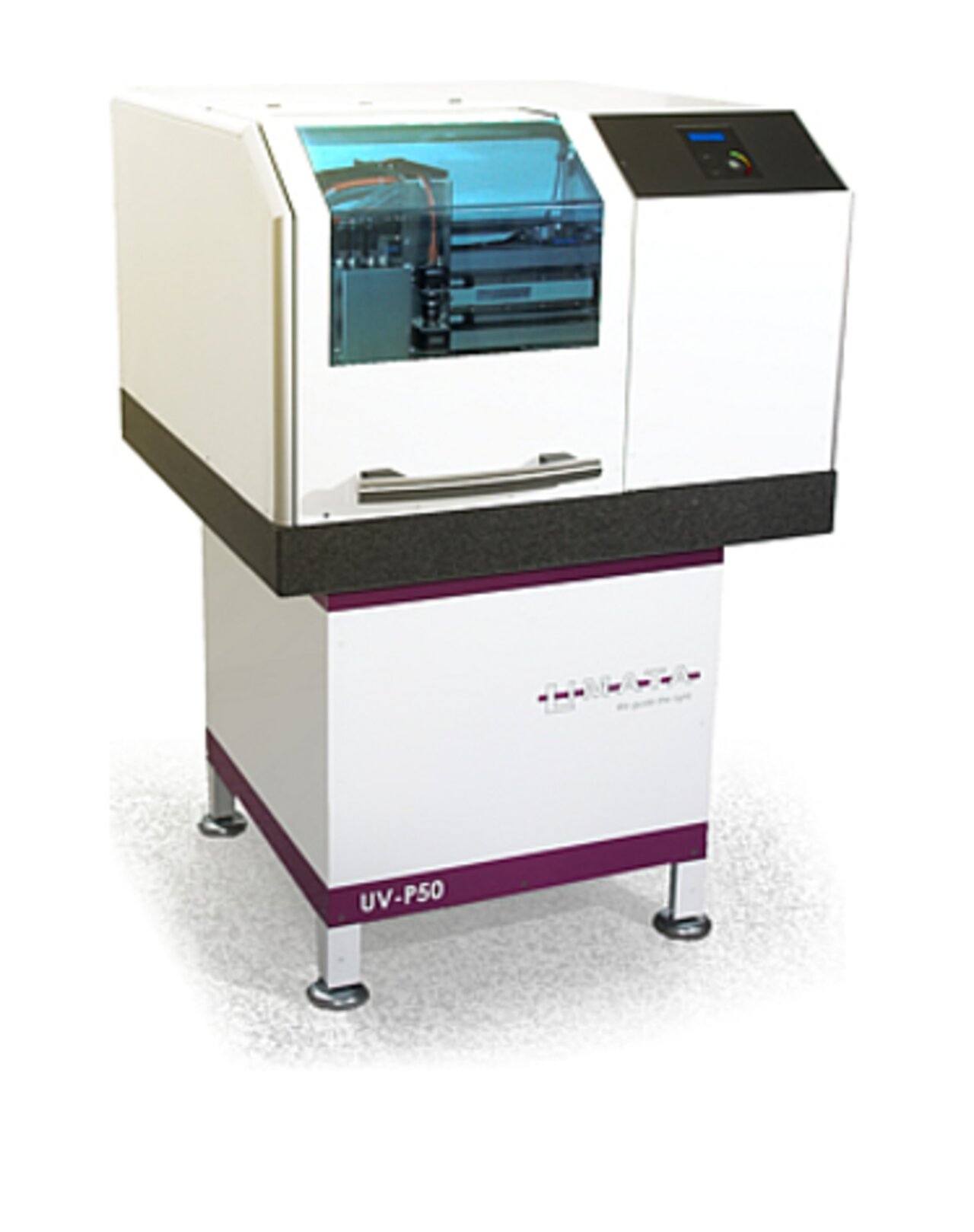
| Panel size (X,Y) | 300 x 400 mm |
| Resoultion | +/- 1 µm (increment), +/- 10µm (repeatability) |
| Minimal conductor track width | 100 µm |
| Material thickness | 0.1 - 10 mm |
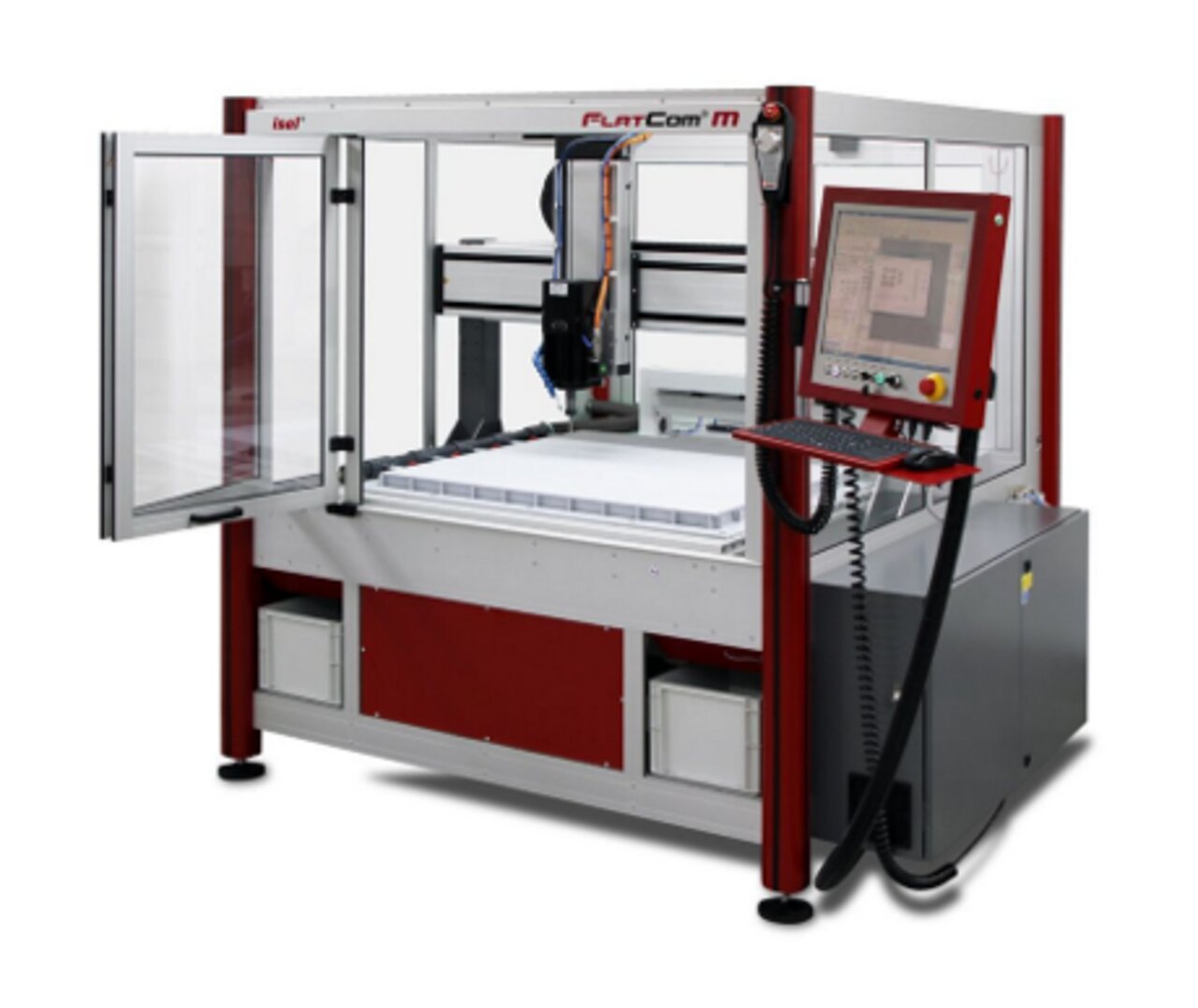
| Clamping surface (T-grooved plate) (X,Y) | 750 x 800 mm |
| Work space (X,Y) | 710 x 500 mm |
| Processing speed X/Y/Z | Max. 250 mm/s |
| Repeat accuracy | +/- 20µm |
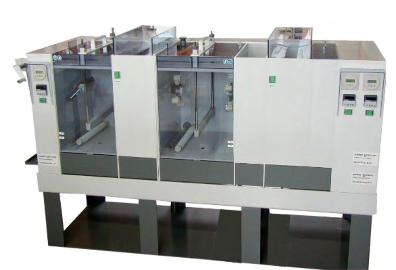
| Workspace (X,Y) | 300 x 400 mm |
| Possibilities | Spray development, spray etching, neutralizing, rinsing and drying single or double-sided printed circuit boards |
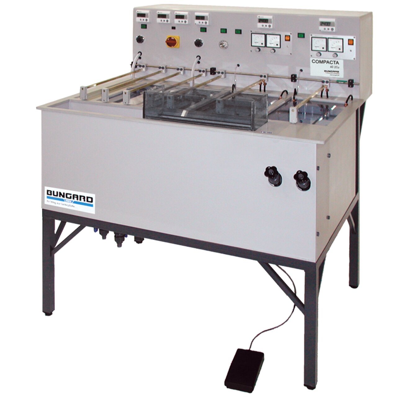
| Printed circuit board size (X,Y) | 300 x 400 mm |
| Filling volume of treatment basin | 20 L |
| Filling volume of galvanized basin | 60 L |
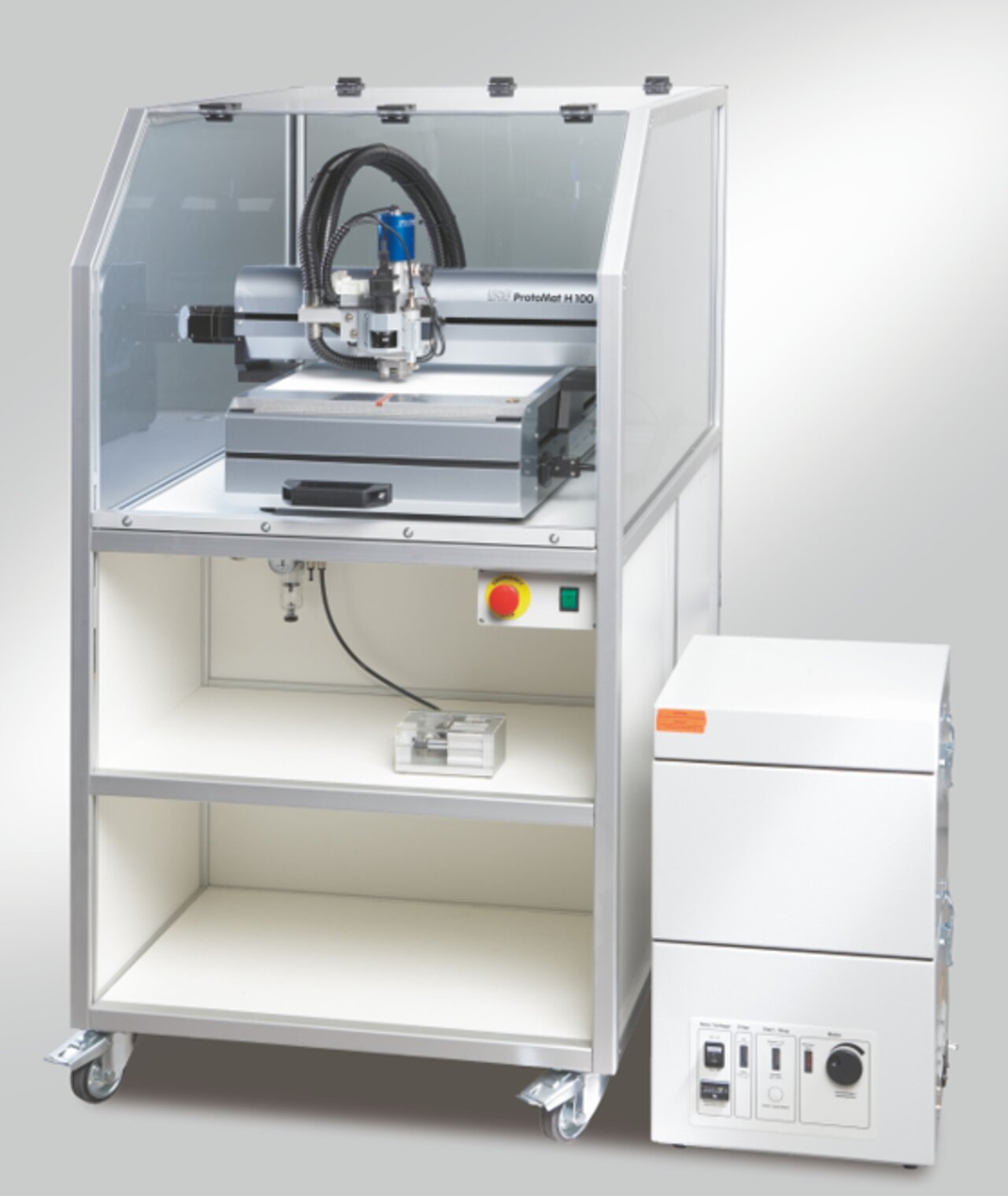
| Workspace (X,Y,Z) | 380 x 365 x 14 mm |
| Resolution | 0.25 µm |
| Repeatability | +/- 1 µm |
| Process speed | 150 mm/ s |