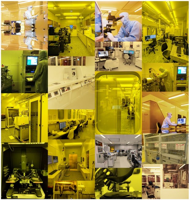

Micro- & nanolithography:
e-Beam-Lithography (Raith Voyager- & eLine Plus EBL), various optical mask- & maskless aligners (Heidelberg MLA100, Süss MA6)
Thin film deposition:
PE-ALD (oxides: Al2O3, SiO2, HfO2, …), PE-CVD (Si3N4, SiO2, SiC, aSi, 2D-materials), spin coating photo resists & polymers
PVD (e-Beam deposition Cr, Au, Ti, Al, Ag, Ni, Co, … & sputtering)
Dry etching:
ICP-RIE (Cl + F, cryo etching, BOSCH), Ar-IBE (multi-layer etching), XeF2 (high selective Si, Ge etching), reactive plasma (O2, SF6, H2)
Substrates & Sample treatment:
Substrates/wafers: Si, Si/SiO2, SiO2, glass wafer - dicing, cleaning, annealing, wet etching, wire bonding
Sample characterization:
Film thickness & stress (ellipsometry, profilometer), SEM, FIB, AFM, optical microscopes (2D, 3D), probe stations