Atomic Layer Deposition (ALD) is a pulsed chemical vapor deposition (CVD) process for depositing thin films or nanoparticles with sub-nm precision in feature size. ALD is based on the sequential exposure of a substrate to gas-phase precursor molecules, which possess the unique characteristic of self-limiting surface chemistry. ALD has emerged as an important technique for thin film depositions, owing to its unique advantages including highly uniform and conformal coverage on high-aspect-ratio substrates and exquisite control of thickness at the atomic level.
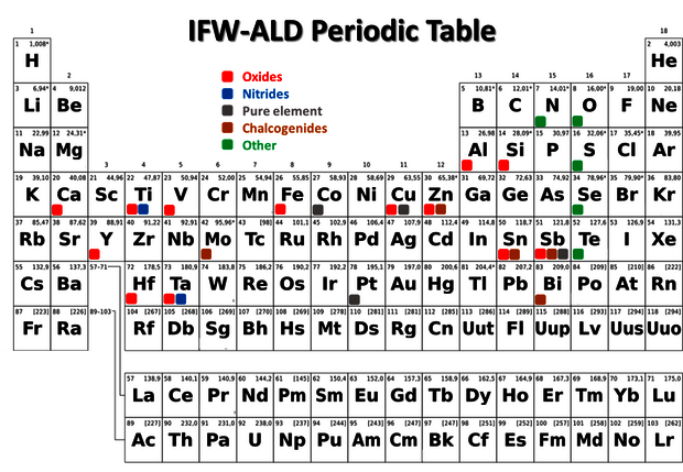
Our group has been working in this area for many years. Various oxide systems, metals, transition metal dichalcogenides, and nitrides have been developed for different applications including but not limited to:
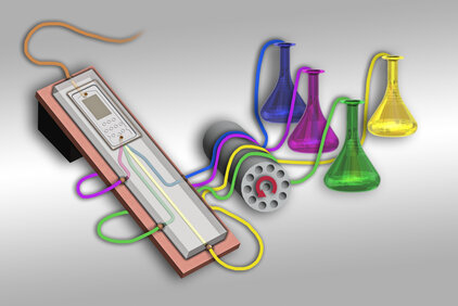
Planar, porous, and powder samples can be coated with the listed materials. Other materials are possible after consultation.
Head of Research Group "Interface Engineering and Atomic Layer Deposition"
Room: A 3E.04.2
Phone: +49 351 4659 104
S. He, S. Lehmann, A. Bahrami, K. Nielsch, Advanced Energy Materials 11 (37), 2101877 (2021)
URL
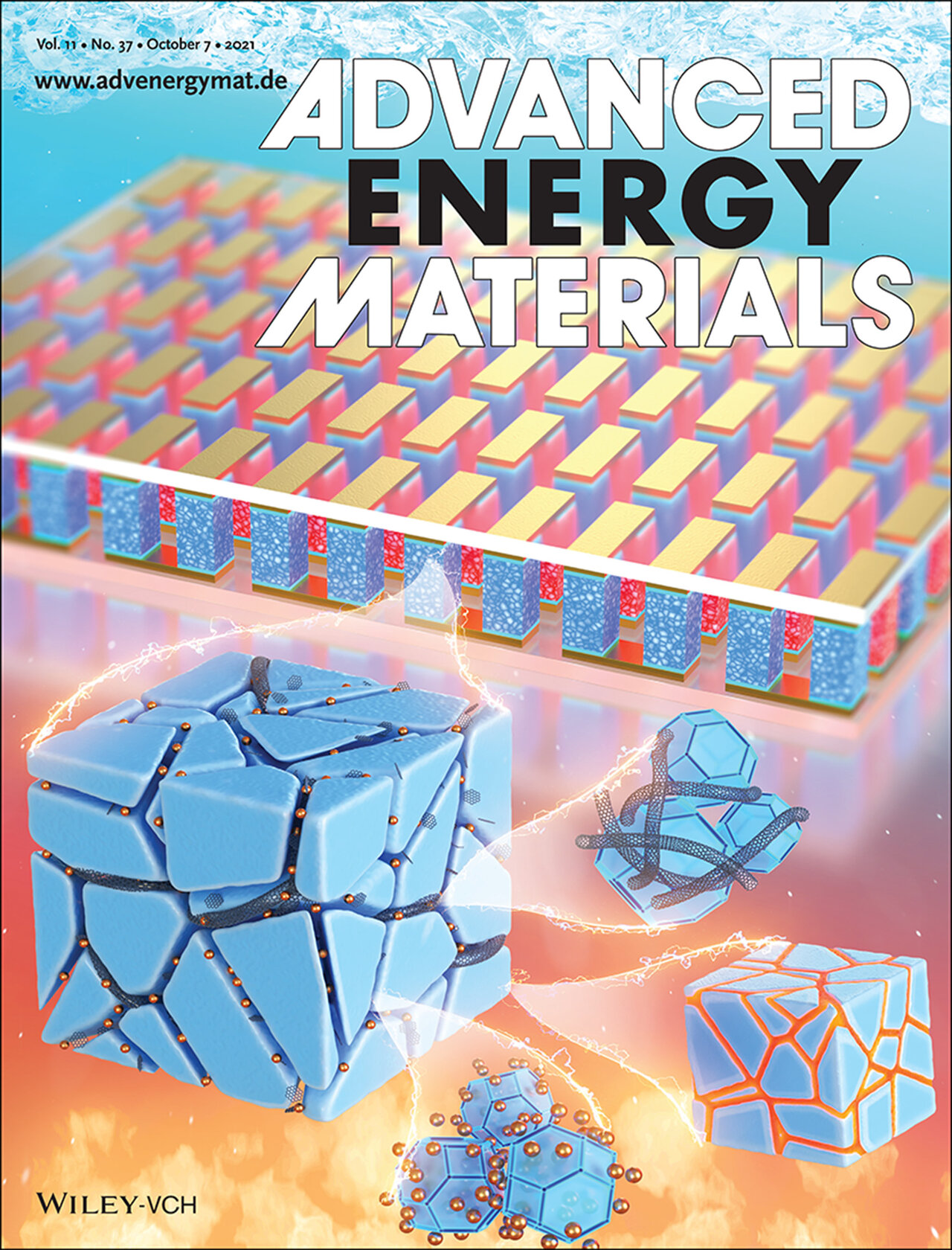
Thermoelectric (TE) materials are prominent candidates for energy converting applications due to their excellent performance and reliability. Extensive efforts for improving their efficiency in single-/multi-phase composites comprising nano/micro-scale second phases are being made. The artificial decoration of second phases into the thermoelectric matrix in multi-phase composites, which is distinguished from the second-phase precipitation occurring during the thermally equilibrated synthesis of TE materials, can effectively enhance their performance. Theoretically, the interfacial manipulation of phase boundaries can be extended to a wide range of materials. High interface densities decrease thermal conductivity when nano/micro-scale grain boundaries are obtained and certain electronic structure modifications may increase the power factor of TE materials. Based on the distribution of second phases on the interface boundaries, the strategies can be divided into discontinuous and continuous interfacial modifications. The discontinuous interfacial modifications section in this review discusses five parts chosen according to their dispersion forms, including metals, oxides, semiconductors, carbonic compounds, and MXenes. Alternatively, gas- and solution-phase process techniques are adopted for realizing continuous surface changes, like the core–shell structure. This review offers a detailed analysis of the current state-of-the-art in the field, while identifying possibilities and obstacles for improving the performance of TE materials.
J. Yang, A. Bahrami, X. Ding, S. Lehmann, N. Kruse, S. He, B. Wang, M. Hantusch, K. Nielsch, Advanced Materials Interfaces 9 (15), 2101953 (2022)
URL
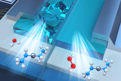
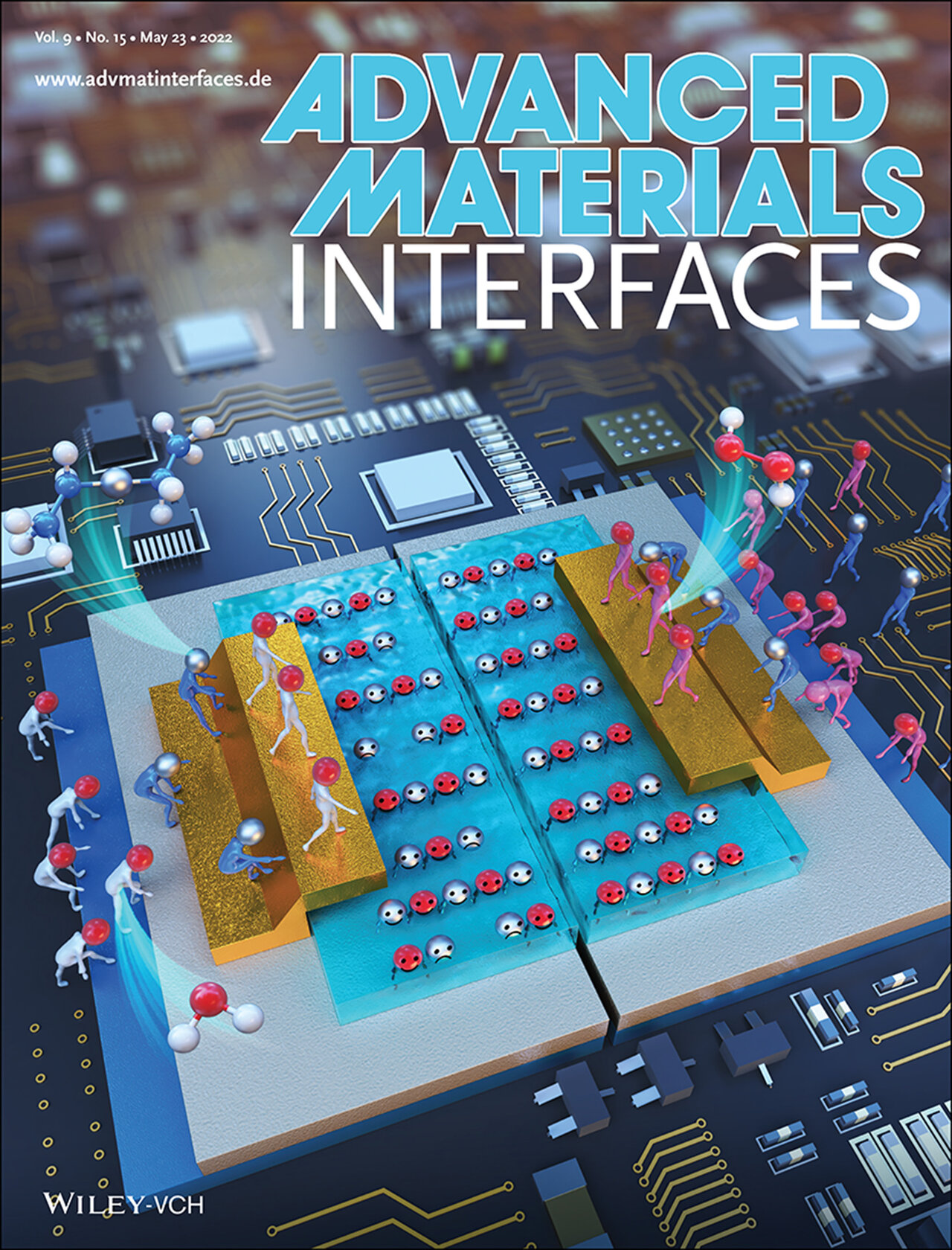
ZnO thin films are deposited by atomic layer deposition (ALD) using diethylzinc as the Zn source and H2O and H2O2 as oxygen sources. The oxidant- and temperature-dependent electrical properties and growth characteristics are systematically investigated. Materials analysis results suggest that H2O2 provides an oxygen-rich environment so that the oxygen vacancies (VO) is suppressed, implying a lower carrier concentration and a higher resistivity. The lower growth rate makes it possible for the ZnO thin films to grow along the lower surface energy direction of <002>, leading to a lower Hall mobility. Furthermore, the ZnO semiconductor is integrated into thin film transistor (TFT) devices and the electrical properties are analyzed. The TFT with H2O2-ZnO grown at 150 °C shows good electrical properties, such as a high field-effect mobility of 10.7 cm2 V–1 s–1, a high ratio Ion/Ioff of 2 × 10⁷, a sharp subthreshold swing of 0.25 V dec–1, and a low trapping state (Ntrap) of 2.77 × 10¹² eV–1 cm–2, which provides a new pathway to optimize the performance of metal-oxide electronics.
S. He, A. Bahrami, X. Zhang, I. G. Martínez, S. Lehmann, K. Nielsch, Advanced Materials Technologies 7 (5), 2100953 (2022)
URL
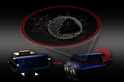
In thermoelectric materials, phase boundaries are crucial for carrier/phonon transport. Manipulation of carrier and phonon scatterings by introducing continuous interface modification has been shown to improve thermoelectric performance. In this paper, a strategy of interface modification based on powder atomic layer deposition (PALD) is introduced to accurately control and modify the phase boundary of pure bismuth. Ultrathin layers of Al2O3, TiO2, and ZnO are deposited on Bi powder by typically 1–20 cycles. All of the oxide layers significantly alter the microstructure and suppressed grain growth. These hierarchical interface modifications aid in the formation of an energy barrier by the oxide layer, resulting in a substantial increase in the Seebeck coefficient that is superior to that of most pure polycrystalline metals. Conversely, taking advantage of the strong electron and phonon scattering, an exceptionally large decrease in thermal conductivity is obtained. A maximum figure of merit, zT, of 0.15 at 393 K and an average zT of 0.14 at 300–453 K were achieved in 5 cycles of Al2O3-coated Bi. The ALD-based approach, as a practical interfacial modification technique, can be easily applied to other thermoelectric materials, which can contribute to the development of high-performance thermoelectric materials of great significance.
Interface Engineering of Thermoelectric Materials Through Powder Atomic Layer Deposition (DFG research grant)
Amin Bahrami (BA 8109/1-1), since 2023
SFB 1415: Chemistry of Synthetic Two-Dimensional Materials - Ferecrystals: Nonepitaxial Layered Intergrowths of 2D Materials by Atomic Layer Deposition (A06)
Kornelius Nielsch (DFG SFB 1415), since 2020
THERMOS - Tellurium-Free Thermoelectric Modules by Interface Engineering
Kornelius Nielsch (IFW, Coordinator), Fraunhofer IFAM (Dresden, Germany), CIC nanogune (San Sebastian, Spain), University of Pardubice (Czech Republic), TEGnology (Soborg, Denmark), SMWK EuProNet M-ERA.NET 2021: 100631228, since 2022