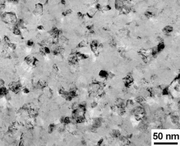
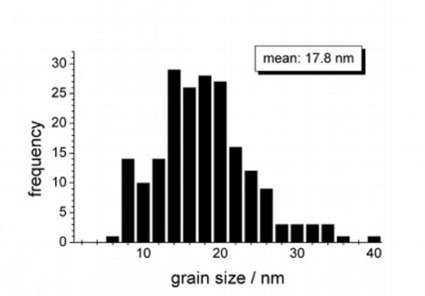
 CTEM image of a grain structure
 Grain size distribution
Basis:
- Mass thickness and mainly diffraction contrast for bright- and darkfield imaging in the fixed beam mode
Possibilities:
- Analysis of morphology of thin films including grain size distribution on the nanoscale
- In-situ observation of crystallisation during heat treatment
- Investigation of lattice defects in crystals
Basis:
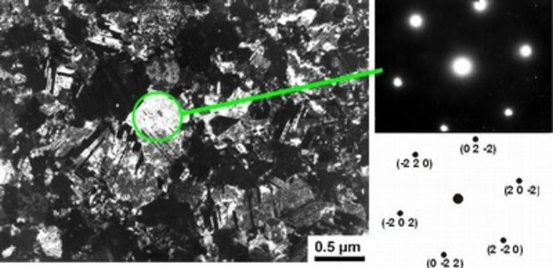
- Interferences of electron waves at crystal lattices
Modes:
- Selected Area Electron Diffraction (SAED)
- Nano Beam Electron Diffraction (nBED)
- Convergent Beam Electron Diffraction (CBED)
Possibilities:
- Phase analysis with correlations to morphological features on the sub-micrometer scale (SAED, nBED)
- Texture analysis (SAED)
- In situ observation of phase formation during annealing (SAED, nBED)
- Determination of lattice parameters with high accuracy on the sub-micrometer scale (CBED)
Basis:
- Phase contrast due to the phase modulation of the electron waves by the periodic crystal lattice
Possibilities:
- Characterisation of interfaces on the atomic scale
- Visualization of nanocrystals in an amorphous matrix
Basis:
- Mass thickness and diffraction contrast for brightfield imaging in the scanning mode
- Dominant Z-contrast for distinction of different materials in High Angle Annular Darkfield (HAADF) imaging
Possibilities:
- Material localization down to the sub-nanometer scale
- Analysis of interfaces down to the sub-nanometer scale
- Combined with EEELS and EDXS: chemical analysis with spatial resolution on the nanometer scale

