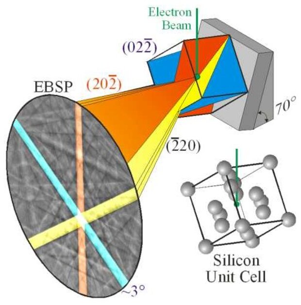
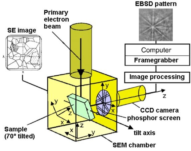
Quick orientation measurements on bulk specimen with high lateral resolution by acquiring and analysing so-called Electron Backscatter Diffraction (EBSD) patterns, (also called Kikuchi patterns).
Requirements for EBSD
- Primary electron beam with high energy (default 20 keV, down to 10 keV possible) and intensity (beam current 0.5nA or more)
- Working distance to SEM polepiece and distance of EBSD detector as low as geometrically possible due to sample size limitations (<= 10mm)
- Specimen steeply tilted (by default 70° , 45° to 80° possible)
- Conductive surface essential, thin carbon coating if necessary
- Flat surface due to tilting, no deformation layer
- metal sections prepared conventionally must be additionally polished to reduce deformation layer (mostly with a nano-sized silica suspension like OP-CHEM)
Characteristics of measurement, possible results:
- lateral resolution down to some ten nm, depending on atomic number
- information depth between 50 and 100 nm
- measured orientations acquired point-by-point in an orientation file automatically
- data can be evaluated without restrictions offline after measurements
- acquisition time 10 to 100 points/second, depending on material/surface quality
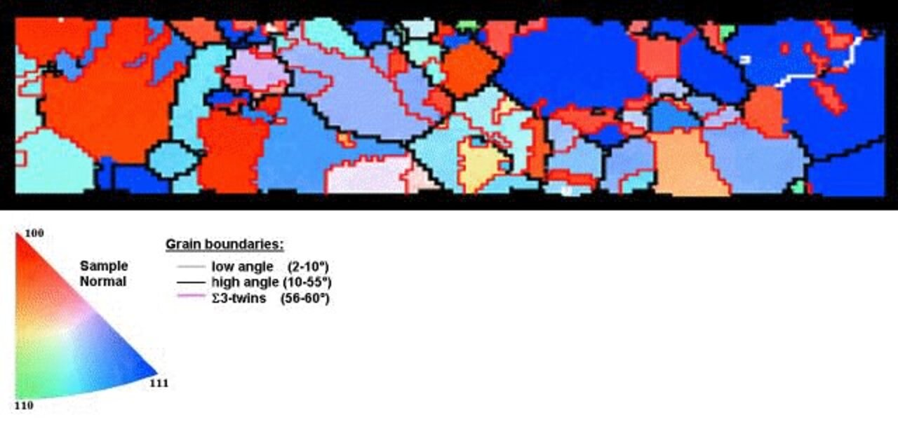
from the data, entire set of microstructure quantities can be obtained:
content of phases, size and shape of grains, misorientation within deformed grains
- grain boundary type (misorientation angle, CSL classification)
- texture results like pole figures, inverse pole figures, ODF, fractions, indices…